CFB
OKI helps improve the added value of semiconductor devices and contributes to the society's well-being by providing CFB (Crystal Film Bonding) solutions.
The Goal of OKI's CFB Solution
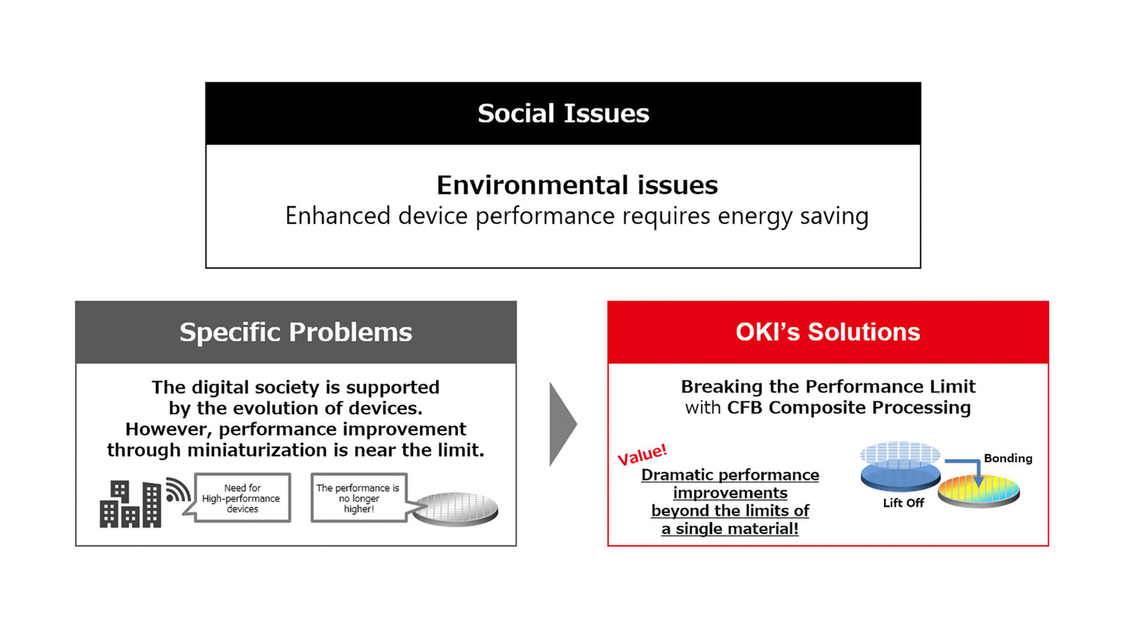
In recent years, efforts toward the SDGs (Sustainable Development Goals) have accelerated, and there is an increasing need to improve the added value of semiconductor devices that support the sophistication of society. As the miniaturization limit of silicon ICs (Integrated Circuits) based on Moore's law is approaching, the trend is shifting towards giving the higher added value of semiconductor devices by incorporating the complexity that integrates disparate functions (More than Moore).
The technology that integrates different devices through the complexity improves the added value by integrating functions that silicon ICs cannot have, such as optical devices, power devices, analog/MEMS devices, etc., so it is attracting attention as the key to driving the sustainable growth of the semiconductor industry.
OKI was the first in the world to successfully mass-produce the CFB (Crystal Film Bonding) technology, which combines LEDs and ICs using a unique bonding technology. Since then, we have shipped more than 100 billion dots of the combined LED elements, which is established as a core technology with high reliability in mass production. CFB solutions contribute to improving the added value by combining semiconductor devices based on the CFB technology.
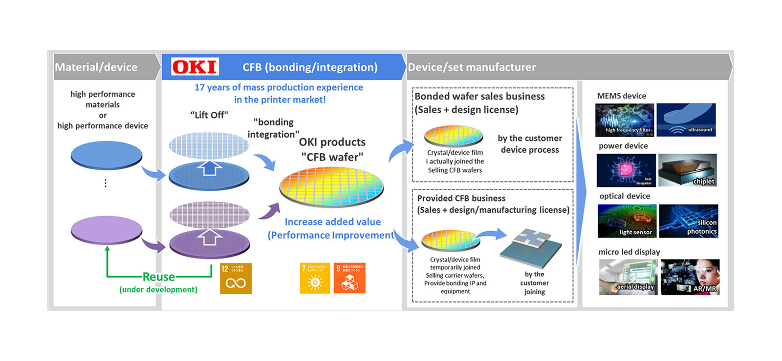
We provide "CFB solutions" that bond dissimilar materials to device manufacturers
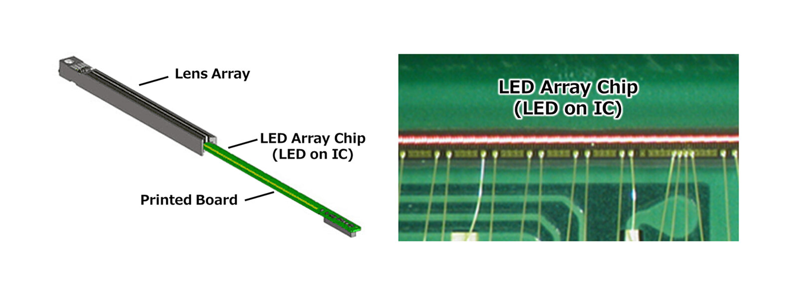
CFB is a technology cultivated in the OKI LED printer business.
"CFB Solutions" is an initiative that extends the CFB technology not only to the LED printer business but also to various crystalline materials and devices, contributing to improving the added value of semiconductor devices. A new added value is created by lifting off a crystalline film (high-performance material, disparate-function device) from a seed substrate, and bonding and integrating them onto different boards.
There are two business models for CFB solutions.
The first is the "bonded-type CFB business," which sells CFB boards in which crystalline films are bonded onto boards made of disparate materials.
The second is the "supply-type CFB business," which provides a license to temporarily bond crystalline films onto carrier substrates and enable a transfer of the crystal films in the customer's process. Supply-type CFB is a type of CFB that overcomes differences in board size and device constraints.
Use Case
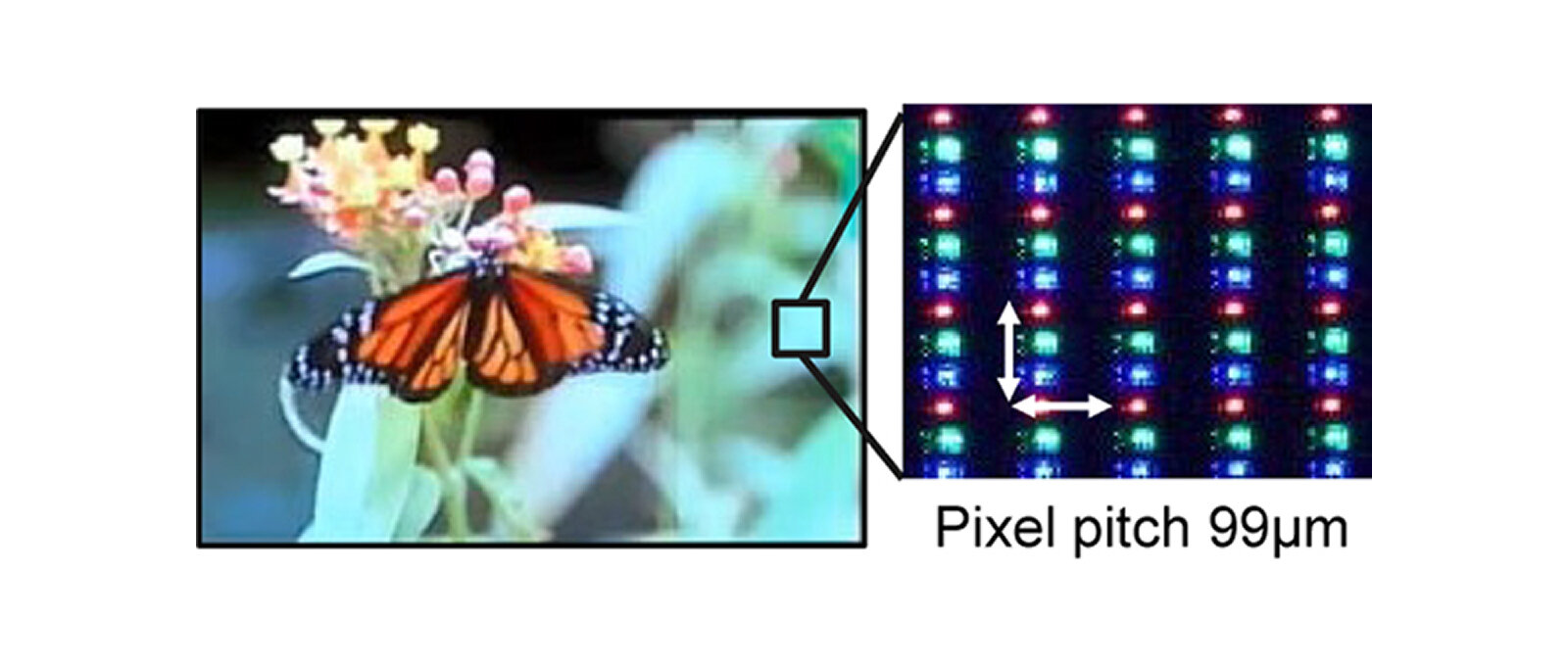
Application to LED Display
In recent years, with the advent of AR (Augmented Reality)/MR (Mixed Reality), there has been an increasing need for smart glasses and head-up displays that allow users to view new business spaces that fuse reality and virtual reality. However, to become more widespread, there are issues such as increasing brightness to increase visibility that enables outdoor use during the day, and reducing power consumption to facilitate use of smaller batteries. The micro LED displays are attracting attention as a means to solve these issues. Micro LED displays are expected to have higher brightness and lower power consumption because all pixels are composed of micro LEDs, which are self-luminous elements.
However, in order to create full color, a large number of micro-LEDs must be bonded together using different materials that emit red, green, and blue (R, G, and B), which poses issue in terms of manufacturing technology. Therefore, OKI has made it possible to solve this manufacturing issue with the CFB solution.
Use Case
Application to MEMS Device
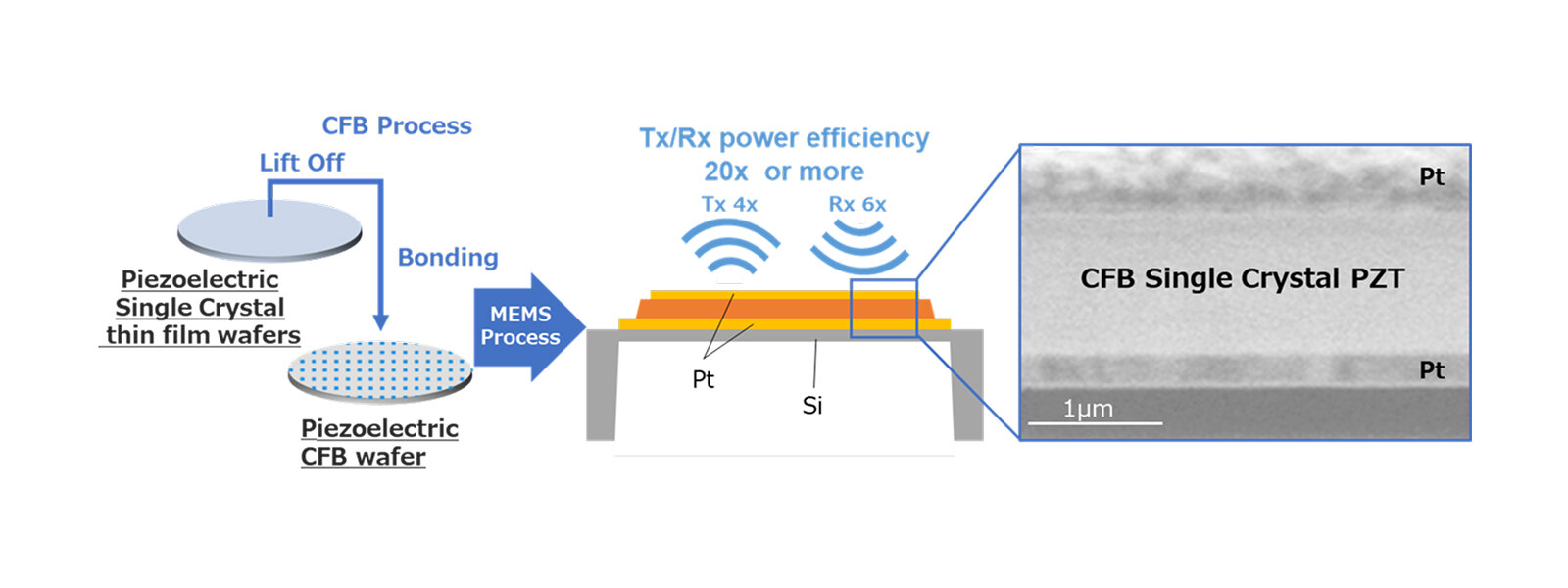
OKI and I-PEX Piezo Solutions Inc. (hereinafter referred to as IPS) (Note 1) have established a bonding technology for piezoelectric single crystal thin films and SOI wafers, and successfully prototyped a "piezoelectric single crystal thin film bonding wafer" that dramatically improves the performance of piezoelectric MEMS devices such as ultrasonic sensors.
Conventional piezoelectric thin films are polycrystalline with the crystals arranged unevenly, so they could not demonstrate the performance inherent to the material. A single crystal with the crystals arranged properly can exhibit its original physical properties, but it has been difficult to form a single crystal in a practical area. Therefore, by using a unique buffer layer, IPS succeeded in producing a single crystal in a practical 8-inch size, achieving the extremely high performance compared to polycrystalline materials.
In this co-creation, we hoped to increase the new added value that could not be imagined previously by lifting off and bonding IPS' piezoelectric single crystal thin films without damaging their performance using OKI's CFB solutions, leading to the co-creation.
Note 1: Company name changed from KRYSTAL, Inc. to I-PEX Piezo Solutions Inc. on January 1, 2023.
Use Case
Application to Power Semiconductor Devices
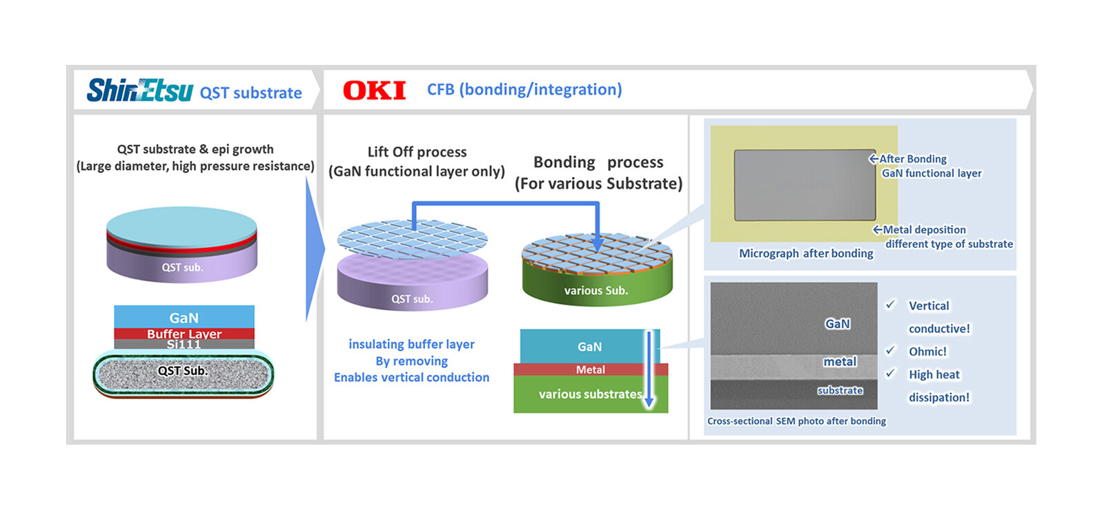
In collaboration with Shin-Etsu Chemical Co., Ltd. (hereinafter referred to as Shin-Etsu Chemical), OKI has successfully developed a bonding technology to lift off only the GaN (gallium nitride) functional layer from Shin-Etsu Chemical's uniquely improved QST substrate and bond it into a different material board using OKI's CFB technology.
This technology enables the GaN vertical conduction, contributing to the realization and widespread use of vertical GaN power devices that can control large currents. In the future, the two companies will continue to develop vertical GaN power devices that can be implemented in society by partnering with customers who manufacture GaN devices.
About CFB's future initiatives
OKI will continue to carry out co-creation with material manufacturers and device manufacturers based on CFB solutions that utilize the CFB technology, and contribute to increasing the added value through composite processing of semiconductor devices. We will also contribute to solving social issues by considering the use of advanced semiconductor materials through CFB solutions.